from d2l import torch as d2l
import time
import torch

torch.set_float32_matmul_precision('high')13.2 Hardware
The previous section introduced a model with two machine parameters. A machine delivers \(\min(P, I\beta)\): peak arithmetic \(P\) when the operation supplies enough work per byte, and bandwidth \(\beta\) times intensity otherwise. This section explains where those two numbers come from, why their ratio — the ridge point — has climbed over the long run of hardware generations, and what else about the machine (latency, capacity, interconnect, energy) a practitioner needs in order to reason about performance before running anything. The aim is enough working knowledge to read a profiler, size a model, and identify an appropriate optimization. For the complementary question — what hardware should I buy — see the buyer’s guide in Section 30.4; this section is about why the machine behaves the way it does, whatever machine you have. For a proper treatment of computer architecture see (Hennessy and Patterson 2011).
The specific hardware values below were verified in mid-2026 and will change with new products. More stable are the ratios and trends: memory is orders of magnitude slower than arithmetic, every chip boundary costs roughly another order of magnitude, and compute grows faster than bandwidth, which grows faster than capacity. The numerical values should therefore be checked for the hardware in use.
from d2l import jax as d2l
import jax
from jax import numpy as jnp
import numpy as np
import time
13.2.1 The Memory Hierarchy
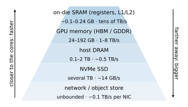
Every byte your program touches lives somewhere in a hierarchy (Figure 13.2.1), and each level trades capacity for speed: small pools close to the arithmetic are fast; large pools far away are slow. On one end sit the GPU’s on-die memories — registers and caches totaling on the order of a tenth of a gigabyte, reachable at tens of terabytes per second. Then comes the GPU’s own DRAM — the high-bandwidth memory (HBM) of datacenter parts or the GDDR of consumer cards — tens to hundreds of gigabytes at one to eight terabytes per second. Host DRAM holds hundreds of gigabytes at a few hundred gigabytes per second; NVMe flash holds terabytes at about fourteen gigabytes per second; and network storage offers effectively unbounded capacity, at whatever your network card delivers.
Two comparisons quantify the hierarchy. Figure 13.2.2 ranks data paths by bandwidth: from an NVMe drive’s 14 GB/s, through PCIe and socket DRAM, up to on-package HBM at 8 TB/s. The span is almost three orders of magnitude, and the levels correspond to physical boundaries: on-package memory is fastest because it sits on the same package, millimeters from the die over thousands of short interposer wires; everything that crosses a connector, a board trace, or a cable reduces available bandwidth. As a rule of thumb, every chip boundary costs roughly an order of magnitude of bandwidth. Performance therefore improves when data remains near the arithmetic units that use it.
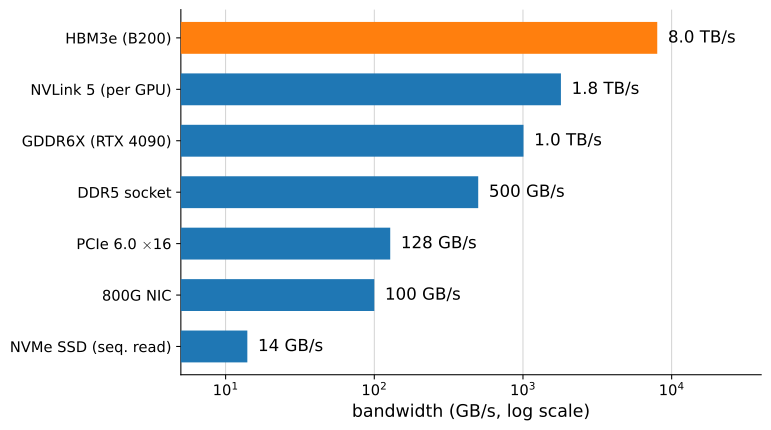
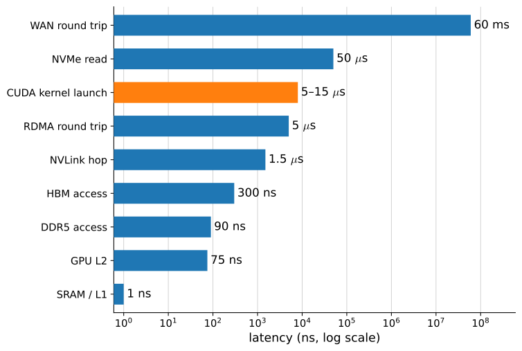
Figure 13.2.3 compares the same systems by latency — how long before the first byte arrives — and spans eight orders of magnitude, from a one-nanosecond L1 hit to a sixty-millisecond WAN round trip. Note where the highlighted point sits: launching a CUDA kernel costs 5–15 µs of latency, thousands of L2 hits’ worth, which is why the overhead regime of Section 13.1 exists at all and why this chapter keeps returning to “fewer, larger operations”.
Latency and bandwidth interact through access patterns. DRAM delivers its rated bandwidth only for burst reads: addressing a location costs on the order of a hundred nanoseconds, after which sequential transfers stream at full rate — so the first word of a random read is hundreds of times more expensive than the words that follow it. Sequential streaming therefore approaches rated memory bandwidth, whereas pointer-chasing does not; caches amortize latency only when access patterns are local and predictable. For dense tensors this is mostly handled for you — a matmul kernel is a carefully choreographed burst-read machine — but it is why sparse and gather-heavy workloads struggle to reach more than a fraction of rated bandwidth, and why shuffled dataset access is best done at the granularity of large blocks. (The classic multi-core pathology of false sharing — two CPU threads bouncing one cache line between cores — is relegated to the exercises.)
Let’s measure the one number from this subsection that matters most for the roofline: our card’s achievable memory bandwidth. A large elementwise scaling reads and writes every element once — bytes moved are known exactly, arithmetic is negligible — so timing it is measuring bandwidth:
x = torch.randn(256 * 1024 * 1024, device=d2l.try_gpu())  # 1 GB fp32
t = d2l.Benchmark(lambda: x * 2.0).time
print(f'measured {2 * x.numel() * 4 / t / 1e12:.2f} TB/s '
      f'(spec: about 1.0 TB/s)')
measured 0.80 TB/s (spec: about 1.0 TB/s)x = jax.random.normal(jax.random.PRNGKey(0), (256 * 1024 * 1024,)) # 1 GB
t = d2l.Benchmark(lambda: x * 2.0).time
print(f'measured {2 * x.size * 4 / t / 1e12:.2f} TB/s '
f'(spec: about 1.0 TB/s)')measured 0.91 TB/s (spec: about 1.0 TB/s)A well-shaped streaming kernel lands within tens of percent of the specification — the spec number is real, not marketing. Remember what this kernel is: a direct measurement of the bandwidth-bound regime. Every elementwise operation in every network you train runs at this speed, no matter how little it computes.
13.2.2 Why Compute Outruns Bandwidth
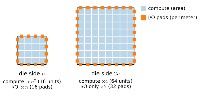
The geometric scaling of compute and I/O explains the ridge point in Section 13.1. Arithmetic units fill the interior of a die: double the die’s side length (or halve the feature size) and you get four times the compute, because compute scales with area. But the wires that leave the chip — the I/O drivers that talk to memory — live on the die’s edge, and the edge only doubles. Compute scales as \(n^2\), I/O as \(n\) (Figure 13.2.4). Chip designers call the edge “beachfront”, and there is never enough of it: bytes-per-FLOP therefore tends to fall across hardware generations.
HBM is the countermeasure: stack DRAM dies vertically and place the stack on a silicon interposer millimeters from the GPU die, so thousands of short, dense wires replace the few hundred long board traces a socketed DIMM gets. That is how a B200 reaches nearly 8 TB/s while a CPU socket manages 0.5 TB/s — not faster DRAM cells, but vastly more, vastly shorter wires. The second countermeasure is size: dies are manufactured against a hard lithographic ceiling (the reticle limit, about \(858\,\textrm{mm}^2\)), and flagship accelerators live at it — a B200 is two reticle-limit dies bridged into one logical GPU. When a die cannot grow further, multiple dies are connected on-package or through a network. Section 13.2.5 examines the resulting bandwidth limits.
The long-run trend to memorize, averaged over many hardware generations at fixed precision: compute grows about \(4\times\) per generation, bandwidth about \(2\times\), capacity about \(1.7\times\). Over the years the ridge point — compute over bandwidth — has therefore risen, and workloads that were compute-bound a decade ago are bandwidth-bound today. Do not expect every product step to obey the average, though: which roof moves faster in any single generation is a packaging and market decision, and it can go the other way. The H100\(\to\)B200 step grew compute and bandwidth almost in lockstep (both about \(2.3\times\) — the ridge point barely moved, in fact edging slightly down), and the consumer 4090→5090 step bought bandwidth far faster than compute, dropping its ridge point by nearly a third — check the ridge row of Table 13.2.1 below. The shoreline sets the long-run pressure; engineering choices determine whether compute or bandwidth improves more in a particular generation. Averaged over the decade, compute wins — which is why a chapter about performance is mostly a chapter about bytes, and why it will remain one.
13.2.3 The GPU
A GPU spends its area on thousands of simple arithmetic units rather than on the deep control logic of a CPU core. The units are organized into streaming multiprocessors (SMs) — our RTX 4090 has 128 of them — and each SM executes threads in lockstep groups of 32 called warps, swapping between many resident warps to hide memory latency. That is as much microarchitecture as this book needs: when a profiler reports “occupancy” it means resident warps available for latency-hiding; when a kernel is “too small for the machine” it means too few warps to keep 128 SMs busy — the launch-overhead regime again.
What makes GPUs deep learning machines is a further specialization: tensor cores, silicon shaped exactly like a small matrix multiply-accumulate. A scalar unit spends most of its energy on instruction handling per multiply; a tensor core amortizes that control over an entire \(16\times 16\)-ish tile, executing it as one instruction — the same insight as the TPU’s systolic array (Jouppi et al. 2017; Kung 1988). The consequence: matrix multiplications run an order of magnitude faster than anything else on the chip, provided the data comes in the formats the tensor cores speak. Figure 13.2.5 compares their bit allocations.
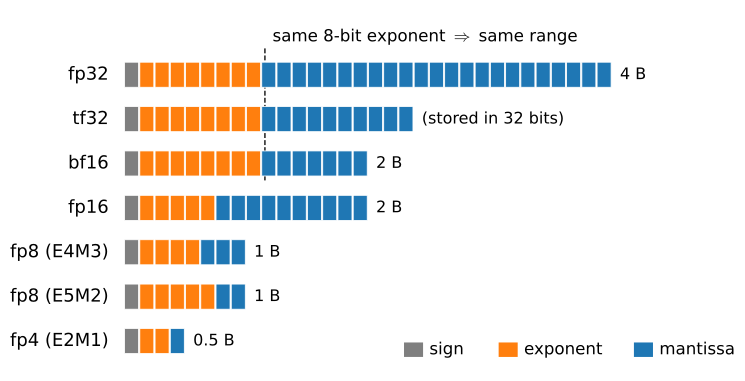
Two rules organize the comparison. First, the exponent width sets the range, the mantissa width sets the precision. fp32, tf32, and bf16 all carry the same 8-bit exponent: they represent the same span of magnitudes, so swapping among them costs precision, not range — you give up decimal places, which deep learning mostly tolerates, rather than the ability to represent a large activation at all. fp16’s 5-bit exponent trades range for precision, which is why it needs the loss-scaling machinery we will meet in Section 13.4, and why bf16 has become the training default. The sub-byte formats push the same trade to its limit and lean on per-block scaling factors to survive (Micikevicius et al. 2022): fp8 comes in two flavors (E4M3 for activations and weights, wider-range E5M2 for gradients, in the usual recipe rather than by any rule), and fp4 has just sixteen representable values. Second, every halving of storage wins twice: half the bits means double the peak FLOP/s (twice the tile fits in the same silicon) and half the bytes per operand — reduced precision moves the roofline bound along both axes at once. tf32 is the exception that proves the byte rule: it is a tensor-core compute format that still stores 32 bits (the figure draws exactly this), so it buys throughput but saves nothing on memory traffic. Each halving yields about \(2\times\) higher throughput on current silicon, not the \(4\times\) suggested by multiplying the compute and storage factors. Larger generational gains also depend on architectural changes.
The numbers-dense table, for orientation (conventions below it):
| H100 SXM | B200 SXM | RTX 4090 (ours) | RTX 5090 | |
|---|---|---|---|---|
| memory | 80 GB HBM3 | 180 GB HBM3e | 24 GB GDDR6X | 32 GB GDDR7 |
| bandwidth | 3.35 TB/s | 7.7 TB/s | 1.0 TB/s | 1.8 TB/s |
| bf16 dense | 989 TF | 2,250 TF | 165 TF | 210 TF |
| fp8 dense | 1,979 TF | 4,500 TF | 330 TF | 419 TF |
| fp4 dense | — | 9,000 TF | — | 1,676 TF |
| ridge (bf16) | ~295 FLOP/B | ~292 FLOP/B | ~165 FLOP/B | ~117 FLOP/B |
| power | 700 W | 1,000 W | 450 W | 575 W |
Conventions: dense throughput (no 2:4 sparsity), fp32 accumulation, boost clocks, vendor datasheets as of mid-2026. The B200 column is the shipping HGX B200 spec; the GB200 NVL72 variant of the same silicon runs 186 GB at 8 TB/s and up to 1,200 W. The 5090’s fp4 entry is \(4\times\) its fp8 entry, not \(2\times\), because GeForce parts run fp8/fp16 tensor math at half rate when accumulating in fp32 while fp4 carries no such penalty.
The same constraints produce the same shape at every vendor — high-bandwidth stacked memory next to a die full of matrix engines: AMD’s MI355X (288 GB HBM3e at 8 TB/s, 2,500 TF dense bf16), Google’s TPU v7 (192 GB at 7.4 TB/s, 2,307 TF), Amazon’s Trainium2 (96 GB at 2.9 TB/s, 667 TF). Different silicon, one design point; the roofline reasoning of this chapter applies unchanged to all of them.
The table does not show a further distinction: training hardware must hold activations for the backward pass and accumulate gradients robustly (bf16 with fp32 accumulation as the floor — Section 13.4), while inference can run forward-only in the smallest format quality allows. That asymmetry shapes the memory anatomy we build in Section 13.4, and so does capacity, which grew the slowest of the three curves.
13.2.4 The CPU’s Role
The CPU in a deep learning machine is no longer where the FLOPs happen — one RTX 4090 out-multiplies a 64-core CPU by two orders of magnitude — but it remains responsible for three performance-sensitive tasks. First, the CPU is the orchestrator: every kernel the GPU runs was launched by a CPU thread at 5–15 µs apiece (Figure 13.2.3), which is the Python dispatch constraint from Section 13.1 — until the capture-and-replay of Section 13.3 takes the CPU out of that loop. Second, it runs the input pipeline: decoding JPEGs, tokenizing text, augmenting, batching — if those operations fall behind, the GPU remains idle regardless of its peak throughput (a dataloader-starved profile is the overhead regime with extra steps). Third, it feeds the bus: host-to-device copies cross PCIe, and how you stage the host memory matters. A regular (pageable) host tensor must first be copied into a locked staging buffer before DMA can move it; allocating the tensor in pinned (page-locked) memory skips that step and, as a bonus, allows the copy to proceed asynchronously alongside compute. How much the staging costs — and who controls it — differs between our two frameworks:
x_pageable = torch.randn(64 * 1024 * 1024)          # 256 MB on the host
x_pinned = x_pageable.pin_memory()
gpu = d2l.try_gpu()
for desc, src in [('pageable', x_pageable), ('pinned', x_pinned)]:
    t = d2l.Benchmark(lambda: src.to(gpu, non_blocking=True),
                      desc=f'{desc} H2D').time
    print(f'{desc}: {x_pageable.numel() * 4 / t / 1e9:.1f} GB/s')
pageable: 13.4 GB/s
pinned: 24.3 GB/s# JAX manages host staging internally; measure the achieved H2D rate.
x_host = np.random.randn(64 * 1024 * 1024).astype(np.float32) # 256 MB
t = d2l.Benchmark(lambda: jax.device_put(x_host), desc='H2D').time
print(f'device_put: {x_host.nbytes / t / 1e9:.1f} GB/s')device_put: 0.9 GB/sPinned memory roughly doubles the pageable rate, and the pinned figure sits near PCIe’s practical ceiling — tens of GB/s, a factor of about forty below the GPU’s own memory. This is why the standard input pipeline asks for both pieces at once: DataLoader(pin_memory=True) to stage batches in pinned memory, .to(device, non_blocking=True) to overlap the copy with compute.
The physical link supports tens of GB/s, yet jax.device_put from a pageable NumPy array lands far below the bus limit — around one gigabyte per second at our pin. The copy is not the cost; JAX’s transfer path (validation, layout, staging through its own host buffer) is, and that is itself the lesson: a transfer runs at the speed of its slowest stage, and the framework owns some of the stages. JAX programs sidestep the problem structurally rather than tuning it — keep arrays resident on the device, let the input pipeline overlap transfers with compute, and treat a per-step device_put of fresh host data as a red flag.
The resulting guideline is to stage data on the device and overlap unavoidable transfers with compute. Inter-device transfers are bounded by the applicable interconnect rather than by local device-memory bandwidth; the multi-GPU sections measure that difference directly.
13.2.5 Interconnects: Our Box as the Worked Example
When one GPU is not enough, devices exchange gradients, parameters, or activations over an interconnect whose bandwidth is usually far below local memory bandwidth. Datacenter parts attack the problem with dedicated fabrics: NVLink gives each B200 1.8 TB/s to its peers — memory-class bandwidth below HBM — and an NVL72 rack wires 72 GPUs into a single 130 TB/s domain. Consumer parts get PCIe, and the current GeForce generations (RTX 40 and 50 series) have peer-to-peer transfers disabled as market segmentation, the fact that shapes the rest of this chapter: two RTX 4090s in one box may not even talk PCIe-directly to each other. (It was not always so — the RTX 3090 still carried an NVLink bridge; its successors dropped it.)
Our build machine makes the consequence concrete (Figure 13.2.6). Its four RTX 4090s hang in pairs off two PCIe host bridges; with P2P disabled, every byte from one GPU to another is staged through host DRAM — up one PCIe link, through the CPU’s memory system, down another. Measured end to end (Section 13.5 does the measuring), a large GPU-to-GPU copy sustains roughly twenty GB/s — PCIe-limited, two orders of magnitude below an NVL72’s ~1.8 TB/s per GPU. A collective library like NCCL extracts even less on this staged path (a couple of GB/s of effective bus bandwidth), because its ring/tree chunking assumes a peer-to-peer fabric and its P2P-less fallback moves bytes with a latency-bound mechanism by default; the wire itself does not slow down for NCCL. Section 13.5 diagnoses this and names the one-line workaround, which Section 13.6 weighs. Either way the staging path, not the link count, sets the ceiling, so the rate does not improve from two GPUs to four.
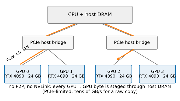
nvidia-smi topo: four RTX 4090s in pairs behind two PCIe host bridges, no P2P, no NVLink. The highlighted path is what every inter-GPU byte actually travels.
This host-staged configuration makes communication costs directly measurable. Most readers’ multi-GPU machines look like ours, not like an NVL72; and a slow fabric makes the accounting of parallel training vivid — on this box, communication costs are impossible to ignore, so the cost model of Section 13.5 predicts real behavior instead of disappearing into NVLink headroom. We will not have to assert why datacenter fabrics exist; we will have measured it.
13.2.6 Energy Cost of Data Movement
Energy provides another comparison. Figure 13.2.7 shows the energy cost of elementary operations at a fixed process node (Horowitz 2014): an 8-bit integer add costs 0.03 pJ, an fp32 multiply 3.7 pJ — and one 64-bit read from DRAM costs about 2,000 pJ. Thus this table assigns one DRAM read approximately the energy of five hundred fp32 multiplies. The exact numbers depend on process and hardware generation, but the ordering explains why data movement is often a primary power and performance cost.
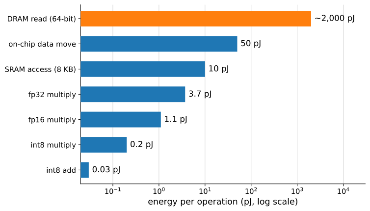
The practical corollaries are the fixes this chapter teaches: fusion (Section 13.3) saves energy, not just time, by keeping intermediates on-die; low-precision formats (Section 13.4) halve the bytes and hence nearly halve the energy per operand; recomputation trades cheap arithmetic for expensive memory traffic. The techniques in this chapter follow the same principle: perform more arithmetic per byte fetched, as quantified by Figure 13.2.7.
13.2.7 Reading the Roofline: Two Workloads
The hardware numbers place one language model in two different performance regimes. Consider a language model of the kind built in Section 11.2, with \(N\) parameters in bf16 (\(2N\) bytes of weights), serving a prompt and then generating.
Prefill — processing the prompt — pushes the whole context through the network at once. Each weight fetched from memory is reused across every token in the context, so arithmetic intensity is on the order of the context length: hundreds to tens of thousands of FLOPs per byte, far above any ridge point. A long, well-batched prefill is therefore typically compute-bound: it runs at the tensor cores’ pace and benefits from every format halving. (A one-line prompt is not — intensity needs context to reuse each weight against.)
Decode — generating one token at a time — is the opposite. Producing a single token performs about \(2N\) FLOPs but must read all \(2N\) weight bytes (plus the KV cache of Section 11.3): intensity \(\approx 1\) FLOP/byte, the bottom of the roofline. Decode is bandwidth-bound, and its bandwidth limit is
\[ \textrm{tokens/s} \;\lesssim\; \frac{\beta}{\textrm{bytes per token}} \;=\; \frac{\beta}{2N + \textrm{KV bytes}}. \tag{13.2.1}\]
An 8-billion-parameter model in bf16 reads at least 16 GB per generated token; on our 1 TB/s card that caps generation near sixty tokens per second regardless of compute, while the same card’s prefill chews through the prompt at tensor-core speed. One model, both ends of Figure 13.1.1 — and the reason batching multiple generation streams is the central trick of inference serving: batching shares each weight read across streams, multiplying intensity by the batch size. The systems that exploit this belong to the Language Models part — batching schedulers, paged caches, speculative decoding — while the economics fit in the equation above.
The following table summarizes the characteristic performance scales:
| quantity | magnitude | why it matters |
|---|---|---|
| kernel launch | 5–15 µs | small ops cannot feed the GPU (Section 13.3) |
| GPU memory bandwidth | 1–8 TB/s | the decode/elementwise speed limit |
| PCIe per direction | tens of GB/s | host\(\leftrightarrow\)device; get data on-device, keep it there |
| NVLink-class fabric | ~1.8 TB/s per GPU | why datacenter multi-GPU scales and PCIe boxes struggle |
| bytes/param, training with Adam | ~16–20 (mixed precision) | memory anatomy of Section 13.4 |
| bytes/token, decode | ~2 × params + KV | tokens/s ≤ bandwidth / this |
| DRAM read vs fp32 multiply | ~500× the energy | fuse, shrink formats, recompute |
13.2.8 Summary
- Memory is a hierarchy: each level away from the arithmetic holds orders of magnitude more bytes and delivers orders of magnitude fewer per second, with the compared latencies spanning eight decades. Bandwidth is earned by streaming; boundaries cost an order of magnitude each.
- Compute scales with die area, I/O with die perimeter. The long-run outcome is compute growing ~4× per generation against bandwidth’s ~2× and capacity’s ~1.7×, so the ridge point has risen over the years — though a single product step can move it either way (B200 and the RTX 5090 both nudged it down by buying bandwidth). HBM-on-interposer is a countermeasure, not a repeal.
- Tensor cores make matrix arithmetic an order of magnitude faster than everything else, in exchange for format discipline: same exponent = same range; every halving of width doubles FLOP/s and halves bytes.
- The CPU orchestrates (kernel launches), feeds (input pipeline), and stages (pinned-memory PCIe copies). Inter-GPU bandwidth on consumer boxes is host-staged and PCIe-limited — tens of GB/s for a raw copy, and only a couple of GB/s of NCCL busbw at its default fallback settings (Section 13.5 finds the binding stage) — one to three orders of magnitude below an NVLink domain, which is why datacenter fabrics exist.
- In the cited 45 nm measurements, a DRAM access costs about as much energy as 500 fp32 multiplies. Fusion, reuse, and recomputation can therefore reduce both data-movement time and energy.
- One model can live at both ends of the roofline: long-context prefill is typically compute-bound, single-stream decode is bandwidth-bound with tokens/s ≲ bandwidth / model bytes.
13.2.9 Exercises
Shoreline countermeasures. Section 13.2.2 names two countermeasures to the shoreline problem: wider memory interfaces and more dies per package.
- A DDR5-6400 DIMM has 64 data wires, each carrying 6.4 Gb/s. An HBM3e stack has a data interface of 1,024 wires, and a B200 carries eight stacks. Compute the bandwidth of one DIMM, the number of DIMMs that supply the 0.5 TB/s of a CPU socket, and the rate per wire that the B200’s 7.7 TB/s in Table 13.2.1 implies. Which factor accounts for the gap between the socket and the B200, the number of wires or the rate per wire?
- A B200 consists of two dies at the reticle limit of \(858\,\textrm{mm}^2\). Treat every die as a square. Compare the total edge length of the two dies, after setting aside one edge of each for the bridge that joins them, with the edge length of a hypothetical single die of twice the area. Then show that \(n\) dies of a fixed area offer an edge length per unit area that does not depend on \(n\).
- The two dies of a B200 act as one GPU. Which traffic does the split move across a chip boundary that a single die would keep on-die? What bandwidth must the bridge carry, compared with the 7.7 TB/s of HBM? Use the physical reason behind the chip-boundary rule of Section 13.2.1 to explain how an on-package bridge can meet this requirement.
Memory sweep time. The sweep time \(C/\beta\) of an accelerator with memory capacity \(C\) and bandwidth \(\beta\) is the time it takes to read every byte of its memory once.
- Compute the sweep time of each GPU in Table 13.2.1.
- A model in bf16 fills a fraction \(f\) of the memory with its weights. Ignore the KV cache, and use Equation 13.2.1 to bound the single-stream decode rate in terms of \(f\) and the sweep time. Which rate does the bound allow for the largest model that each GPU can hold?
- Under the long-run growth rates of Section 13.2.2, by what factor does the sweep time change per hardware generation? What does this factor imply for the decode rate of the largest model that fits on each new generation?
Format halving on the roofline. Model the step from one format to a format of half its width, as Section 13.2.3 describes, by a doubling of the peak arithmetic \(P\) and a halving of the bytes that every operation moves.
- Use Equation 13.1.2 to compute the speedup of an operation of intensity \(I\), and show that it does not depend on \(I\).
- For a skinny matrix product with batch size \(B\) and \(b\) bytes per element, Equation 13.1.1 approximates the intensity by \(2B/b\). Using Table 13.2.1, find the batch size at which this product becomes compute-bound on the B200 in bf16, fp8, and fp4, and on the RTX 5090 in the same three formats.
- Use the result of the first sub-problem to explain the pattern in the batch sizes of the previous sub-problem, and identify the entry of Table 13.2.1 that breaks the pattern. What does that format step buy a bandwidth-bound operation, and what does it buy a compute-bound one?
Latency hiding. ● Little’s law (Little 1961) states that in a steady state the average number of requests in flight equals the throughput times the average latency of one request. For a memory system, the bytes in flight therefore equal the bandwidth times the latency.
- Take the HBM access latency of Figure 13.2.3, 300 ns, as the latency of a load on the RTX 4090, with its 1.0 TB/s and 128 SMs. How many bytes must be in flight to sustain the rated bandwidth? If every thread has one 4-byte load outstanding, how many warps per SM must be waiting on memory at any moment?
- Repeat the byte count for the B200 at the same latency. Bandwidth grows about \(2\times\) per generation, while DRAM latency has stayed nearly constant for decades. What does this imply for the parallelism that a kernel must expose on each new generation?
- In pointer chasing, the address of every load comes from the previous load, so a chain of loads has one request in flight. A CPU has the DDR5 access latency of Figure 13.2.3, 90 ns, and fetches 64-byte cache lines. Compute the bandwidth of one chain and the number of independent chains that would saturate a socket with 0.5 TB/s.
Starved input pipeline. The compute of a training job alone would process 2 GB/s of decoded images. One worker process prepares batches by running two stages in sequence. It reads compressed JPEG files from NVMe in shuffled order at 1 GB/s of compressed data, and it decodes them on one CPU core at 0.3 GB/s of decoded output. Decoding expands the data eightfold. The training loop then copies each decoded batch from pageable host memory to the GPU at 12 GB/s before it computes on the batch.
- At what rate, in decoded bytes, does one worker deliver batches? Which stage binds, and what would a drive with twice the read rate change?
- Workers run in parallel on separate cores. How many workers keep the GPU fed?
- With enough workers, the synchronous copy still lengthens every training step. By what fraction does it lengthen the step, and by what fraction after a switch to pinned memory at twice the pageable rate? What does an asynchronous copy change?
Ridge point of a link. The ridge point \(P/\beta\) of Section 13.1.1 applies to any data path, with \(\beta\) the bandwidth of that path: it counts the FLOPs that a device performs in the time one byte crosses the path.
- Compute \(P/\beta\) in bf16 for an RTX 4090 against its own memory and against the host-staged GPU-to-GPU path of Section 13.2.5 at 20 GB/s. Compute it for a B200 against its HBM and against NVLink at 1.8 TB/s.
- In data-parallel training (Section 13.5), every GPU holds a copy of a model with \(N\) parameters and processes \(T\) tokens per step at about \(6N\) FLOPs per token. The GPUs then sum their bf16 gradients with an allreduce, a collective operation that sends about twice the gradient bytes from every GPU. Assume that compute runs at peak and does not overlap communication. Show that communication takes no longer than compute exactly when \(T\) exceeds a threshold proportional to the ridge point of the link, and that the threshold does not depend on \(N\).
- Evaluate the threshold for the host-staged path, for NVLink, and for an effective 2 GB/s, the rate that NCCL reaches on the staged path of Figure 13.2.6 at its default settings. By what factor does the ridge point of each of these links exceed the memory ridge point of the same GPU? Relate the factors to the chip-boundary rule of Section 13.2.1.
Energy per byte. Use the energies of Figure 13.2.7, and charge every FLOP the energy of one fp32 multiply.
- Find the arithmetic intensity at which the energy of the arithmetic equals the energy of reading its operands from DRAM, and compare it with the ridge point of the RTX 4090. What limits the time of an operation with an intensity of 100 FLOP/byte, and what dominates its energy?
- A B200 is rated at 1,000 W and streams 7.7 TB/s from HBM. Compute the power that this traffic would draw at the DRAM energy of Figure 13.2.7, and the largest energy per byte that the power rating allows. Explain the discrepancy with the packaging of Section 13.2.2.
- An 8-billion-parameter model in bf16 decodes on a B200 at the bound of Equation 13.2.1, ignoring the KV cache, while the card draws its full 1,000 W. Compute the energy per generated token and the electricity cost of one million tokens at 0.30 US dollars per kWh. Repeat for 64 streams that share every weight read, after checking that the batched step is still bandwidth-bound.
Launch-bound decode. In eager single-stream decode, the CPU launches every kernel of every block for every token, while the GPU reads the weights of every block. Consider a GPT whose \(L\) blocks of width \(d\) each hold about \(12d^2\) weights in bf16 and launch \(K = 12\) kernels per token. Take 8 µs per launch, from the range of
Figure 13.2.3. Launches are asynchronous, so a decode step takes at least the larger of the total launch time and the time to read the weights. Ignore the embedding table and the KV cache.
- Show that which of the two times is larger does not depend on \(L\), and find the width \(d^*\) at which they are equal on the RTX 4090 and on the B200.
- Evaluate both bounds on the decode rate of the GPT-2 configuration of Section 11.2.4, with \(d = 768\) and 12 blocks, on the RTX 4090. Which bound binds?
- What does the change of \(d^*\) from the RTX 4090 to the B200 imply for the payoff of the capture-and-replay of Section 13.3 on faster GPUs?
[code] Latency and bandwidth, measured. A transfer of \(n\) bytes over a path with latency \(\alpha\) and bandwidth \(\beta\) takes about
\[t(n) = \alpha + \frac{n}{\beta},\]
so it reaches half the bandwidth at \(n_{1/2} = \alpha\beta\). The model describes a call that is timed to completion on its own, so every measurement below waits for the device after each call.
- Predict \(n_{1/2}\) for the elementwise kernel
x * 2.0of Section 13.2.1, counting the bytes it reads and writes, with \(\alpha\) the kernel-launch latency of Figure 13.2.3 and \(\beta\) the bandwidth that the code of that subsection measures on your GPU. - Time
x * 2.0for tensors from 1 MB to 2 GB, and plot the achieved bandwidth against the size on logarithmic axes. Identify the regimes that the curve passes through, and relate the sizes at which it changes regime to Figure 13.2.3 and to the on-die capacity in Figure 13.2.1. In which regime does the curve depart from \(t(n)\), and why? - Repeat the host-to-device measurement of Section 13.2.4 for transfers from 4 KB to 256 MB, and fit \(\alpha\) and \(\beta\). Where does the fitted \(\alpha\) fall on Figure 13.2.3?
- Predict \(n_{1/2}\) for the elementwise kernel
[code] Burst versus random access. ● Let
xbe the 1 GB vector of Section 13.2.1, and gather it through an index vectoridxof the same length, asx[idx].- Time the gather with
idxa random permutation and withidxthe identity permutation, which request the same elements in a different order. Report the achieved bandwidth of each, counting the index, the gathered elements, and the output, and the ratio of the two. - Compare the ratio with the cost that the address-setup model of Section 13.2.1 assigns to a random read. Explain the difference with the resident warps of Section 13.2.3.
- Permute blocks of \(k\) consecutive elements instead of single elements, for \(k\) from 1 to 1,024, and plot the bandwidth against the block size in bytes. At what block size does the shuffled gather approach the identity gather? What does this size imply for the granularity of shuffled reads from a dataset?
- Time the gather with
[code] False sharing. ● CPUs keep their private caches coherent at the granularity of a cache line: before a core writes to a line, the copies of that line in the caches of other cores are invalidated. Write a C program in which two POSIX threads each increment their own 64-bit counter \(10^8\) times with a relaxed atomic add (
atomic_fetch_add_explicitfromstdatomic.h). Place the two counters \(s\) bytes apart in one array whose start is aligned to 256 bytes (_Alignas(256)), so that the first counter begins a cache line.- Time the program for \(s = 8\) and \(s = 256\), and explain the ratio with the coherence rule.
- Sweep \(s\) from 8 to 256 bytes. At which separation does the slowdown disappear? Compare it with the cache-line size that the operating system reports for your CPU.